the alpha syntauri system
  a ancient synthisizer concept for the Apple II
   Page No.:H212-2b
 
          the Apple II interface card of the alpha syntauri - later version  
      The interface of the alpha syntauri in the Apple II is rather simple due to the fact that it only passes over the information from the internal decoder interface
 inside of the keyboard. Up to the moment it seems that one part of the information is a parallel set of the 8 Databits. And it seems that at the other hand
some part of the information might be some kind of handshaking and probably some kind of Interrupt-handling.
Unfortunatly this part of the information is not complete because the alpha syntauri system i have purchased from ebay did not
have this interface card. The only information availiable, was taken from only 2 pictures that i had in former days.

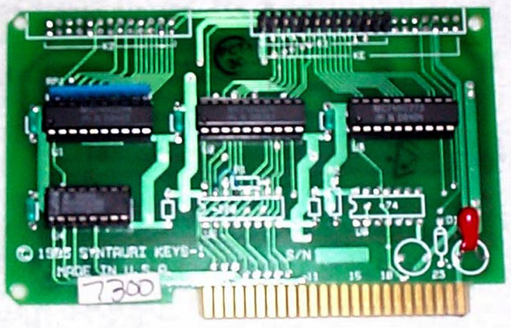
At the beginning just a important remark:
During the time of distribution of the alpha syntauri system, the system has changed several times with several revisions. The information
provided here cover the most common more later ( but not last ) revision of the system I try to research also information on later and earlier
revisions at the moment.
The moment such information gets accessable, i will add such informations to the currently blank pages of this series of pages.

Like with most topics iīve recognized endurance to be one of the most powerfull skills......

The above displayed bad picture of a damaged interface card was for more than 4 years the only info i had on the kind of interface.

Now finally after that period of time i recieved last month a message at applefritter asking if Iīm the author of this site and offering me
information and support for examination of the final bit of unrevealed stuff at this topic and finally enable me to uncover the last mystery
of this system. My special thanks adress to Mr. Charles Hobbs, who passed over the "missing link" by making dozends of pictures and

answering a big bunch of questions about details of this Interface card.


      The pictures below have been made by Mr. Hobbs and display a working version of this interface card with the small misfit that pin1 at the
Connector K1 is broken and is to be repaired. I just enhanced the pictures a bit by correcting perspective and lighting. The left picture displays
the component side while the right picture displays the same card at the soldering side.


Component side soldering side
 
     
Unfortunatly after removal of the Chips it turned out that most sockets didnīt permit very well examination of the traces below of the sockets and that would have required a large amount
of testing measurements to detect the correct connections.
I was therefor very happy that Mr. Hobbs decided to desolder the sockets and send me a second set of pictures of the card with extracted sockets.
This permitted me to recreate the entire shematic ( electronic circuit plan ) of this interface card. I also added this information to the documentation
PDF-file at the end of this section so that in future everybody me be enabled to carry out repairs at the system and at this card.
 
     
card with extracted chips but remaining sockets card with desoldered sockets
 
     
For identification of several components and details Mr. Hobbs has taken several more pictures that offered more details of the card.


After i had the pictures i started working with Photoshop and converted colors to alter the pictures that way that at the end from both sides a kind of clean
negativ film resulted for each side of the interface card and i used the blue color for traces at the component side of the interface card and red for the soldering side of the card.
 
     
Here is the data of the original card:


Here traces at componentside :       here a view of traces at solderside :


Here display of combined view of traces of both layers:      here a view ro components:


In case of damage here are the informations needed for replacement of this card:


traces at the component side   traces at the soldering side


Mounting both layers together gave me a very clear impression of all the connections at the interface and enabled me to recreate the entire schematic.
The picture at the right side just displays the location of the components.


Both Layers ( componentside and solderside ):       PCB sith components:
    
 
      From the reverse engineered replacementcard above the PCB manufacturer files:


as zip-file: ASIFCGerber_mm.zip  ( This files are used with measurement in Millimeter > mm ! )


as rar-file: ASIFCGerber_mm.rar   ( This files are used with measurement in Millimeter > mm ! )


Resulting from this work now finally the picture below displays the complete schematic and the values of the used components like given at the original interfacecard.


In ext part of this page are the function diagrams of the used chips and i sorted them in the same order they are placed at the interface card an i explain
below the chips that are used at this card and the function they perform there at this card. While this order is given by the location on the card it does

not order the the chips by their given order in the explaination.

Explaining the operation of the card :
We will start with the 74LS138 at the bottom row and left side
and next then the 74LS368 in the bottom row at the center, followed
by the 74LS374 in the top row at the center and

then the 74LS273 in the top row at the right and
finally from the top row at the left the  74LS244

followed at the end by the 74LS74 in the bottom row at the right side.

Itīs therefor recommended to read the explaination of the chips in the box
below of the chip in the order given by this previous listing !


74LS244 - a bus transciever

This controller controls 8 Bits of  either data bus
or adressing bus.
In this card the chip controls a data bus  consisting of 8 bits and  that bits are displayed
either at the connectionplug to or from the keyboard
or at the 74LS374

or the 74LS273
and at the 74LS368.

The "activation" of this chip is controlled by O6 output
( pin 9 ) of the 74LS138 which is selected by specific softwareadress at the appleslot.


At this card you may view the Databus consisting of the 8 Databits as a highway with 2 lanes:


1st  lane is from Appleslot to the 74LS244 and the along the 74LS273 to the rearplug connector K2
and the
2nd lane is rather direct from rearplug connector K2 along the 74LS374 towards the appleslot.

The control lines are 1G and 2G.
The 1G line controls the 4 bits from 1A1 to 1A4

and 2G line controls the 4 bits from 2A1 to 2A4.
If the contol-lines recieve a digital "low" signal
then the input signals from 1A1 to 1A4 are
transmitted to the output lines 1Y1 to 1Y4

and the input signals from 2A1 to 2A4 are transmitted
to the output lines 2Y1 to 2A4.

If the control-lines 1G and 2G are at digital "high" level  then the transmission between the input-lines and the output lines at this chip are locked up and disabled.


74LS374 - Octal D-Type Flip-Flop with 3-State Output


At this card you may view the Databus consisting of the 8 Databits as a highway with 2 lanes:


1st  lane is from Appleslot to the 74LS244 and the along the 74LS273 to the rearplug connector K2
and the
2nd lane is rather direct from rearplug connector K2 along the 74LS374 towards the appleslot.


The SN74LS373 consists of eight latches with 3-state outputs for bus organized system applications. The flip-flops appear transparent to the data (data changes asynchronously) when Latch Enable (LE) is HIGH.
 

When LE is LOW, the data that meets the setup times is

latched. Data appears on the bus when the Output Enable (OE) is LOW. When OE is HIGH the bus output is in the high impedance state.


The SN74LS374 is a high-speed, low-power Octal D-type Flip-Flop featuring separate D-type inputs for each flip-flop and 3-state outputs for bus oriented applications. A buffered Clock (CP) and Output Enable (OE) is common to all flip-flops.


The SN74LS374 is manufactured using advanced Low Power Schottky technology .


Eight Latches in a Single Package

3-State Outputs for Bus Interfacing

Hysteresis on Latch Enable

Edge-Triggered D-Type Inputs

Buffered Positive Edge-Triggered Clock

Hysteresis on Clock Input to Improve Noise Margin

Input Clamp Diodes Limit High Speed Termination Effects


74LS273 - a bus latch cotroller


All Databit lines of this chip have connection to the rearplug connector ( pins 3 to 10 ) and may be assumed to be treated as real Dataport from / to keyboard and the Applebus at the slot.


This databits are that portion of information that will be

interpreted as information of the pressed key at the dataport

- opposite to that portion of databits that might be interpreted

as commands between keyboard and interfacecard and

appleslot that explain the devices, how to use the dataport

databits ( like keep a tone for a duration of time stored in a

chip for echo effect ..... ). This chip may keep databits taken

from the dataport dependent to the status of the clock-pin or
the clear-pin in temporary storage and display that stored

values for a period of time - until databit content is deleted by

pulse at the clear-pin  !


This function of storing databits is partially also served by the  74LS74 RS-FlopFlop.

That gate stores a value of the command in it's FlipFlop that portion of time - till it get's reseted by a command-bit from the appleslot -

to be precise : from the reset-pin

or the IRQ-pin ( interrupt request ) of the appleslot

or by adressing selection from the 74LS138.


74LS138 - a multiplexer chip used as  3 Bit - decoder 
First a short explaination of the chipfunction:
Depending from the Gates E1 to E3 this chip decodes

the condition at the gates A0 to A2 and switches one

of the lines from O0 to O7 down to digital "low" status.


The control input E1 is connected to the pin 21 of the connector K1 / K2 at the top of the card and that gets

itīs signal from the keyboard - in other words this line acts like a "hey iīm here present" - signal from the keyboard, if it gets digital "high" signal.


The control input E2 gets itīs signal from the Apple II

slot from pin 41 = Device select and that signal only

gets a digital "high" signal from the Apple - if the

current IO-adressingrange is selected from the

software indicating, that the software wants to talk

with the card.


The 3rd control line E3 is just tied to the 5 Volt rail

and therefor permanent in digital "high" status and
permanent active.


In other words: the chip only decodes the status of

the A0 to A2 ( or if you prefer : the current selected adress within the valid adressing range of the
card ) if the card is selected by the Device-select

signal of the Apple II slot and at the same time gets

the "hey, iīm here present" signal from the pin 21 at

the keyboard connector.

In that case it looks up at the A0 to A2 and decodes

the 3 lowest bits of a byte and switches one of the 8 Output ports O0 to O7 to digital "low"-signal and

thereby activates one of the 3 Bus control chips

in the top row :

either the 74LS244 or the 74LS374 or the 74LS273.


In case of operation of the 74LS138 the so called

truth-table below indicates the results of the

decoding process:

Recognize that only 4 adresses from the
8 possible adresses
are valid at this card
due to the fact that only
O3 to O6 are wired to the chips on the card and only the O3 to O6 wire that is active "low" is really selected !

The relevant adresses are:
Cn00 + 3 ( activates the 74LS368
                 and the 74LS74 )
Cn00 + 4 ( activates the 74LS273 )

Cn00 + 5 ( activates the 74LS374 ) and
Cn00 + 6 ( activates the 74LS244 ).


74LS368 - a bus transciever chip with inverting output of 6 bits.


Due to the fact that at this chip the input-pins
4, 6, 10 and 12 are tied up to 5 Volt ( "High" -signal )

their output lines are also fixed to a defined level.

Pin 14 is in general also tied up to High-level by the 10 k resistor

and only drops to low- signal if it is pulled down by

the pin 4 of the testing plug K3 ( that 6-pin block ).


So in fact only the value at pin 2 and pin 3 are variable.

This results to only 2 different possible status values

that may become presented to the other chips and
may be understood as a kind of switching between
2 different commands  that trigger the other chips.

This commands are triggered by the 2 control-lines
1G ( pin 1 )
and 2G (pin 15 ). In fact pin 15 is tied
to "low"-level ( the GND-line) .
So in fact it's only the signal from pin 12 of the 74LS138
that triggers both ( 74LS368 and 74LS74 ) at the same time - if the software passes a specific adress to the 74LS138 from the appleslot.


Itīs function is also dependent in conjunction with the RS-FlipFlop in the 74LS74.
Due to this fact the databits at this chip must be
valued not as regular data but instead as a kind of
"command-bits" that control the communication of

the interface and thereby the communication between applebus and the keyboard.


74LS74 - a chip with 2 RS flip flops that may store 1 bit for a temporary short period


In this schematic you may value the CP-line ( pin 3 ) as the line

that is used like an input control.


It get's the instruction from pin 12 of the 74LS138 by the adressing

set at the 3 input lines of the 74LS138 given from the appleslot and the software and only at one specific adress the pin 12 of the 74LS138 is triggered.


The output of the 74LS74 is the Q-pin ( pin 5 ) - that passes

the pin 1 of the 74LS368 and then is presented to the rest of

the other chips > from pin 3 of the 74LS368.


       due to european laws and german court decision:
 I hereby declare no responsibility to any "deep links" resulting from the links in this page. I have no influence to the pages linked hereby in this page and the
 contents in those pages. I therefor canīt take any kind of responsibility to contents in the pages, where these links direct the readers browser to nor to the
 contents resulting from following up links from those pages. The reference to contents by this links is dependent ro the status of the date when the links have
 been set ( April 2013 ) and it might occur that references and contents may change by the fact that domains may have been discontinued from their former owners.
 In such cases i canīt take any kind of responsibility to the changed contents. this is specialy valid to banners, advertisements or merchandising links in the targeted
 pages.