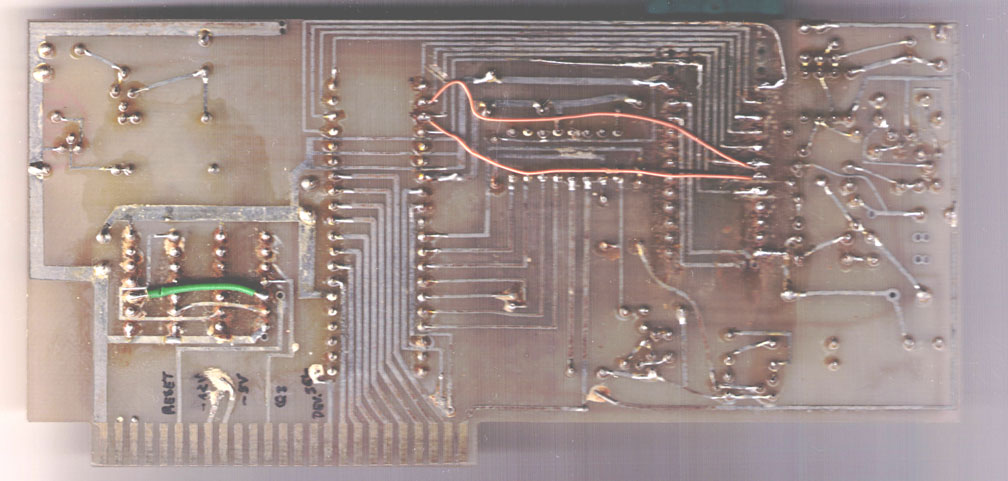
The Springmann Eprom-programmer    Page No.:H051


  The eprom-programmer from Springmann was in the former days of the Apple II+ in Europe a common interface for read and write of the common eproms
  of those days. It was able to handle the 2708, 2716 and the 2732. It was never updated to handle also the 2764 and eproms with 28 pins were never
  supported. That was also the reason why it was distributed only with a 24 pin zero-force socket or in some versions with the 28 pin zero-force socket
  the upper 2 pins at both sides were closed with 2K glue.

  In the distribution pack there was only a plug added for the 2708 and the user was demanded to solder the requested plugs for the 2716 and the 2732
  by himself.


bottomview:

 It seems that the PCB was not made by professional
 PCB - service but seems to be rather more a kind of
 "homebrew" product. Even the points where a
 contact-through is desired a piece of wire was
 soldered in to make sure that at both side a contact
 is given. At the other hand in those days only very
 customers were targeted by the card and it seems
 clear that they never expacted more than 250 to 300
 cards to be sold....
topview:

  The card was designed to only program the most
  common types of eproms ( 1979 to 1980 ) so at that
  days the 2764 was not introduced to the market and
  therefor this card did not support the larger eproms
ī with 28 pins like the 2764 or 27128.

  As far as i know also the software was never updated.
Parts on Board:


  In this picture the values of the components have
  been added. The values in this picture together
  with the componentlabels in the next picture enable
  the reader to identify every component in the later
  following pictures and circuitplans and use then
  components with the exact same values.....

  Here again the PCB as drawing with colored groups of components
  and sorted by Componentlabels:


  In this picture the components have been labeled
  with identifiers. Together with the values of the
  components listed in the picture above every
  component listed later in the circuitplans is exactly
  specified in unique manner. The different colors are
  used to group components together at logical
  parts.
 

  Here are the traces from the backside of the PCB:


  This is the backside of the card and the traced layer.

  Here are the traces from the frontside of the PCB:


  This picture shows the traced layer on the top of the
  card. It took quite a while to find out the correct   
  connections with a multimeter, due to the fact that
  i of course didnīt want to destroy the card and
  several traces are beneath the sockets.

  the both pistures on this page are in lower resolution,
  but in the PDF-documents the pistures are in high
  resolution.

  Though some of the readers might probably use the
  pictures to generate a reproduction of the PCB in a
  software like kiCAD to get a PCB made with one of
  common PCB-services ( such a PCB would be made
  as a trialedition for something about $ 50,00 ) i want
  to take another way in this pages: the circuitary on
  the PCB is rather simple and i want to try to make
  an alternate PCB that is only single sided and therefor
  can be etched with simple amateur-equipment. As
  connection to the appleslot a old damaged card
  or a used experimantalcard may be used.

  The German "manualpages"
 

 First Page:  Second Page:  Third Page:  PDF-File:

 
 German
 Manual


   The translated english text of the "manual"

  First Page :   Second Page :   Third Page :  PDF-File :
     

  english
  version


  Here are the lines of the databus:

   For better understanding i divided the circuitplan
   in several pages with function groups.


   In a few days i will also add commented
   explenations to each group.

  Here are the lines of the adressbus :
  - recognize the text in the picture that explains
    why the lines for adressing are only between
    8255 chip and the programming socket.


  the adresslines that are really used from the
  appleslot are used only for controlling the
  card and they are displayed in the trace of the
  controlling / decoding lines.

   Here is the tracing of the part that generates the
   programming voltage by "switching-technic"
   of the NE555 and 4 transistors as a kind of
   "step-up controller" .... 
   the other 2 transistors are used for switching
   on / off  the programming voltage in alternate read
   or program mode.


        not complete yet !  
         
       due to european laws and german court decision:
 I hereby declare no responsibility to any "deep links" resulting from the links in this page. I have no influence to the pages linked hereby in this page and the
 contents in those pages. I therefor canīt take any kind of responsibility to contents in the pages, where these links direct the readers browser to nor to the
 contents resulting from following up links from those pages. The reference to contents by this links is dependent ro the status of the date when the links have
 been set ( April 2013 ) and it might occur that references and contents may change by the fact that domains may have been discontinued from their former owners.
 In such cases i canīt take any kind of responsibility to the changed contents. this is specialy valid to banners, advertisements or merchandising links in the targeted
 pages.